SPECIFICATIONS
Part No.: IS200JPDSG1ACB
Manufacturer: General Electric
Country of Manufacture: United States of America (USA)
Temperature: -30 to +65oC (-22 to +149 oF)
Agency approval: Class 1 Division 2 explosive atmosphere
Size: 16.51 cm high x 17.8 cm wide
Product Type: Power Distribution Board
Availability: In Stock
Series: Mark VIe
Functional Description
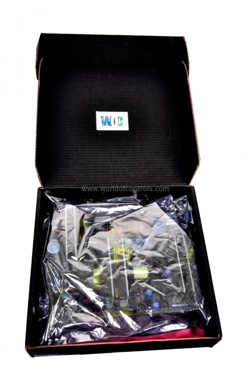
IS200JPDSG1ACB is a Power Distribution Board developed by GE. It is a part of the Mark VIe control system. The board is affixed to a sturdy sheet metal framework, providing a stable mounting platform. It is specifically designed to accommodate a PPDA I/O pack, which is secured onto the board. Within the board, three distinct 28 V DC power buses are incorporated, each with its own dedicated bulk power supply input. For situations requiring a single bus with multiple power supplies, barrier screw terminals are provided to connect the power buses accordingly. While most output circuits do not feature fuses, exceptions are made for three auxiliary circuits. Notably, the design of the JPDS board relies on the current limit of the connected power supplies to ensure protection for branch circuits. Communication between the JPDS and PPDA is facilitated through ribbon cable connections, enabling the exchange of crucial system feedback such as DC bus voltage, power supply status contact feedback, and auxiliary circuit status.
Installation
- Mounting Options: JPDS can be mounted using either a vertical DIN-rail holder or a direct mounting metal holder.
- Wiring Guidance: Refer to provided wiring diagrams for proper routing of power inputs and outputs.
- Diagnostic Connectors: A 50-pin diagnostic connector is present on both the top and bottom of the board for diagnostic purposes.
Operation
- Power Input: The standard power input is through three connectors JR, JS, and JT. These connectors serve as the entry points for the 28 V DC power received from the selected power supplies.
- Distribution to Components: Once the power is received, JPDS efficiently distributes it to the boards, which in turn provide power to the I/O packs. Ensures that the control racks receive the necessary power for their operation.
- Role in System Functionality: As a critical component of the power distribution system, it plays a vital role in ensuring the uninterrupted operation of various subsystems within the larger control system. Its efficient distribution mechanism helps maintain system stability and reliability.
- Importance of Proper Functioning: Given its central role in power distribution, it's essential to function correctly. Any issues could potentially disrupt the power supply to crucial components, leading to system malfunctions or failures. Regular maintenance and monitoring of JPDS are therefore necessary to ensure optimal system performance.
I/O characteristics
- Power Input Connectors: Three connectors, namely JR, JS, and JT, serve as the entry points for 28 V power input. Each power supply connector includes two connections for positive and three connections for negative power. Additionally, three power supply health inputs per power source offer two dry contact inputs each, which transform into diagnostic signals.
- DC Outputs for Rack Control: Three DC outputs, designated as JCR, JCS, and JCT, are provided to control rack CPCI power supplies.
- Outputs to JPDP Cards: Six outputs are allocated to JPDP cards via six-pin connectors (J1 to J6), each following the 3x2 Mate-N-Lok configuration. These connectors, sharing pin assignments with those on the JPDP, allow direct connection of up to six JPDL boards to JPDS to supply I/O packs.
- Auxiliary Power Outputs: Three outputs, labeled JAR, JAS, and JAT, are dedicated to auxiliary power connectors. Each connector includes a positive temperature coefficient fuse for current limiting and features a common-mode choke for noise suppression.
- Internal 28 V Bus Access: Screw terminals on TB1 and TB2 provide access to the internal 28 V bus at the top and bottom of the board. Terminals for R, S, and T can handle a maximum continuous current of 35 A and can be utilized for jumpering boards together. The ground screw terminal is designed for 75 A.
- Diagnostic Interface: A DC-62 connector facilitates connectivity with the PPDA power diagnostic I/O pack. The PPDA monitors JPDS along with up to five additional power distribution boards connected to JPDS using a 50-pin diagnostic ribbon cable.
- P28 Power Output: The P4 output is diode ORed for the PPDA power diagnostic pack.
The WOC team is always available to help you with your Mark VIe requirements. For more information, please contact WOC.
Frequently Asked Questions
What is IS200JPDSG1ACB?
It is a power distribution board developed by GE under the Mark VIe series.
Where is the typical mounting location for the board?
The board is typically mounted in a metal holder that fits onto a vertical DIN-rail alongside other power distribution boards. Optionally, JPDS can also be acquired with a metal holder designed for direct mounting.
Are diagnostic connectors available on the board?
Yes, there are 50-pin diagnostic connectors mounted on both the top and bottom of the board, facilitating diagnostic procedures and connectivity.
How is the board grounded?
The board is grounded through the sheet metal bracket to the underlying back base. In most cases, this base can be the system FE.
