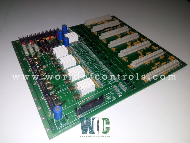
World Of Controls understands the criticality of your requirement and works towards reducing the lead time as much as possible.
DS200VPBLG1ADD - VME Backplane Board is available in stock which ships the same day.
DS200VPBLG1ADD - VME Backplane Board comes in UNUSED as well as REBUILT condition.
To avail our best deals for DS200VPBLG1ADD - VME Backplane Board, contact us and we will get back to you within 24 hours.
Part No.: DS200VPBLG1ADD
Manufacturer: General Electric
Country of Manufacture: United States of America (USA)
Temperature Operating: -30 to 65oC
Product Type: VME Backplane Board
Availability: In Stock
Series: LCI
DS200VPBLG1ADD is a VME Backplane Board developed by GE. It is a part of LCI (Load Commutated Inverter) series. It is designed to serve as the backplane for the J2 and J3 sections of the equipment’s card cage, while the J1 section uses a commercially available product. The board's multilayer architecture separates analog and digital power planes, ensuring minimal interference and reliable performance.
Step 1: Power Down
Ensure the system’s power supply is turned off completely to prevent any electrical hazards.
Step 2: Disconnect Cables
Carefully detach all cables, handling different connector types appropriately:
Step 3: Remove Daughter Boards
Detach all daughter boards following their respective removal procedures as outlined in their documentation.
Step 4: Unscrew and Remove the VPBL Board
Remove the screws securing the VPBL board and carefully slide it out while keeping it level to avoid damage.
Step 5: Configure the New Board
Set all jumpers on the replacement board to match the jumper settings of the removed board.
Step 6: Install the New VPBL Board
Insert the new board into the slot and secure it using the screws provided.
Step 7: Reinstall Daughter Boards
Reconnect all daughter boards by following their specific installation guidelines.
Step 8: Reconnect Cables
Reconnect all cables, ensuring they are properly seated at both ends.
The WOC team is always available to help you with your LCI requirements. For more information, please contact WOC.
What is DS200VPBLG1ADD?
It is a VME Backplane Board developed by GE under the LCI series.
What is the primary function of the board?
The board acts as a communication and power distribution hub for the components installed in the J2 and J3 sections of the card cage. It ensures separate analog and digital power planes for optimal system performance.
What connections are established in the J3 section?
Current Transformers (CTs) and associated burden resistors, Voltage Scaling Feedback Board connections, It also facilitate power connections and various grounding schemes.
What precautions should I take while handling the board?
Power off the equipment before starting. Handle connectors and cables gently to avoid damage. Ensure the board is kept level during removal and installation. Prevent hardware from dropping onto the board or into the equipment.