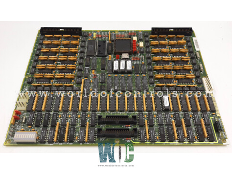
World Of Controls understands the criticality of your requirement and works towards reducing the lead time as much as possible.
DS200TCDAG2BBA - Digital I/O Board is available in stock which ships the same day.
DS200TCDAG2BBA - Digital I/O Board comes in UNUSED as well as REBUILT condition.
To avail our best deals for DS200TCDAG2BBA - Digital I/O Board, contact us and we will get back to you within 24 hours.
Part Number: DS200TCDAG2BBA
Manufacturer: General Electric
Series: Mark V
Product Type: Digital I/O Board
Operating Temperature: 0 to 60oC (32 to 149 oF)
Availability: In Stock
Country of Manufacturer: United States (USA)
DS200TCDAG2BBA is a Digital I/O Board developed by General Electric. It is a part of Mark V system. Designed to process digital contact input signals and contact output (relay/solenoid) signals. The Digital I/O Board (TCDA) is located in the digital I/O cores Q11, Q51, and Q21 (if present). Its primary function is to receive digital contact input signals from the DTBA and DTBB terminal boards. Transmit contact output (relay/solenoid) signals to the TCRA boards. Communicate signals over IONET to the TCQC board in R1 and R2 (if Q21 is installed) and the CTBA terminal board in R5.
The board includes eight hardware jumpers for configuration:
WOC has the largest stock of Speedtronic control spares. Please contact our staff by phone or email for pricing and availability on any parts and repairs
What is DS200TCDAG2BBA?
It is a Digital I/O Board developed by General Electrics.
Where is TCDA located?
The board is located in the digital I/O cores Q11, Q51, and Q21 (if present) of the Mark V control system.
How is the TCDA configured?
It has eight jumpers for IONET ID, termination resistors, and stall timer enable settings.
Jumpers J1 and J8 are for factory testing. I/O configuration constants are used to manage contact input signal inversion via the HMI.
What is the role of the JX1 and JX2 connectors?
Both JX1 and JX2 serve as IONET signal transmission connectors. Either one can be used to send signals to TCEA (P1 core) or CTBA (R5 core).