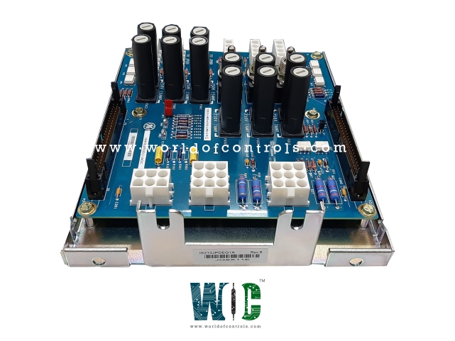
World Of Controls understands the criticality of your requirement and works towards reducing the lead time as much as possible.
IS210JPDEG1A - DC Battery Power Distribution Terminal Board is available in stock which ships the same day.
IS210JPDEG1A - DC Battery Power Distribution Terminal Board comes in UNUSED as well as REBUILT condition.
To avail our best deals for IS210JPDEG1A - DC Battery Power Distribution Terminal Board, contact us and we will get back to you within 24 hours.
TECHNICAL SPECIFICATIONS:
Part Number: IS210JPDEG1A
Manufacturer: General Electric (GE)
Series: Mark VIeS
Product Type: DC Battery Power Distribution Terminal Board
Board Form Factor: Compact Power Distribution Module
Total Board Rating: 30 A total dc
Fuse for Connectors JS1-JS3: FU11-12, FU21-22, FU31-32
Input Voltage: 24 V DC / 125 V DC Power Distribution Branches
Circuit Protection: Onboard Fuses with LED Blown-Fuse Indicators
Power Output Channels: Multiple Fused Output Branches for Control & Field Power
Terminal Block Type: Fixed Screw Terminal Blocks for Power Cabling
Connectors: Ribbon Cable Headers & Multi-Pin Power Connectors
Board Dimensions: 16.51 cm High x 17.8 cm Wide (6.5 in x 7 in)
Operating Temperature: -30°C to +65°C
Storage Temperature: -40°C to +85°C
Relative Humidity: 5% to 95% Non-Condensing
System Compatibility: GE Mark VI Turbine Control & Innovation Drive Cabinets
Availability: In Stock
Repair Lead Time: 3–7 Days
Country of Origin: United States
Manual Reference: GEH-6721_Vol_II_BP
The IS210JPDEG1A is a Power Distribution Terminal Board designed and manufactured by General Electric as part of the Mark VIeS Series and Innovation Series drive and control systems. The JPDEG1A board receives dc power from a battery or power supplies and distributes it to terminal boards and other system loads. JPDEG1A supports a floating dc bus that is centered on earth using resistors and provides voltage feedback through PPDA to detect system ground faults. It provides inputs for two power supplies. JPDEG1A is able to operate at either 24 V dc or 48 V dc.
JPDEG1A integrates into the PDM system feedback offered through the PPDA I/O pack. This board is limited by the current that can be passed through it using conventional board construction. JPDEG1A does not supply power to bulk 500 W - 24 V input/28 V output power supplies providing I/O pack control power. JPDEG1A is the PDM element that receives dc power from a battery or power supplies and distributes it to I/O such as relay and contact input boards. JPDE supports a floating battery bus that is centered on earth using resistors, and provides voltage sensing to detect system ground faults. It provides inputs for two power supplies including their associated status contact feedback. The design is compatible with applications using either 24 V or 48 V dc.
INSTALLATION:
The current that can be passed through the board (using conventional board construction techniques) limits the amperage capabilities of this board. For this reason, the JPDE is not intended to supply power to bulk 500 W 24 V input / 28 V output power supplies providing I/O pack control power. Each one of these supplies will consume approximately 25 A at full load. A set of three for R, S, and T would then use 75 A, exceeding the conventional capability of circuit boards. While special board construction is possible to address the high current, the resulting high product cost would exceed the cost of using simpler and readily available commercial components. When power distribution is needed for I/O, it is more functional to have a board that provides centering resistors for a floating bus, voltage feedback for magnitude and ground detection, status feedback from dc power supplies, and fused output monitoring. The JPDE addresses these needs.
JPDEG1A GROUNDING:
Mark VIe control systems separate ground into a functional earth (FE) and a protective earth (PE). The protective earth is intended for power distribution functions such as JPDE, while functional earth is used for quiet uses such as the control electronics and field signals. Grounding of the JPDEG1A takes place through metal mounting standoffs. The ground is applied to the metal switch bodies on JPDE. In addition, the ground is used as a local reference when creating the magnitude feedback signals appearing on P2.
JPDEG1A PHYSICAL ARRANGEMENT:
JPDEG1A is designed to accept power input from the right-hand side and deliver power output from the left-hand side. The P1 and P2 ribbon cable headers on all of the JPDx boards are designed so the JPDS or JPDM holding the PPDA I/O pack is best located at the top of the arrangement. This allows ribbon cables to flow from one to the next, exiting the top and entering the bottom of the next until the PPDA host is reached.
JPDEG1A CONNECTIONS:
JD1 is a 6-pin Mate-N-Lok connector that accepts power input from a battery. Three connector pins are used for positive and negative connections to provide an adequate current rating.
JFA, JFB, and JFC are fused four-pin Mate-N-Lok output connectors. Positive power is on pins 1 and 2, and negative power is on pins 3 and 4. This matches the pin usage on JPDD J28 and J28X. These connectors have a fuse rating of 15 A.
JP1 is the ground reference jumper. The dc bus is normally operated without a hard ground connection. The dc bus is centered on earth as part of the ground fault detection scheme. Normally, the 24 V operation of the dc positive terminal would measure 1⁄2 * 24 V above ground, and the negative terminal has the same magnitude below ground potential. Resistors to center the bus on earth are supplied externally to the JPDE, or on-board resistors can be used by closing jumper JP1.
JPS1 and JPS2 are nine-pin Mate-N-Lok connectors used for power supply input. The connector uses pins 8 and 9 for positive 24/48 V dc and pins 1-3 for 24 V return, providing 24 A steady-state capacity. Pin 4 provides positive 10 V dc wetting to a supply status feedback switch, and pin 5 provides the return.
JS1, JS2, and JS3 are fused and switched four-pin Mate-N-Lok output connectors. Positive power is on pins 1 and 2, and negative power is on pins 3 and 4. This matches the pin usage on JPDD J28 and J28X. The fuse rating for these switched connectors is 7 A.
Two 50-pin diagnostic ribbon cable connectors, P1 and P2, are supplied on the top and bottom of the board. Connector P1 transmits feedback signals to a board hosting a PPDA I/O pack. Connector P2 receives feedback from other power distribution boards and passes the signals to P1 to the PPDA.
WHY BUY FROM WOC
World of Controls maintains an extensive global stock of genuine OEM replacement parts for GE Mark VIeS and Innovation Series control systems. The JPDEG1A Power Distribution Board is available in UNUSED surplus and fully REBUILT conditions, covered by complete warranty protection. Every unit undergoes comprehensive inspection and electrical bench testing by experienced technical personnel to verify fuse holder continuity, voltage bus isolation, terminal integrity, and surge circuit health prior to dispatch. We also offer fast repair and exchange services to help power generation facilities prevent costly downtime. Contact our sales team today to check live stock, request a quote, or arrange quick worldwide delivery.
What is the GE IS210JPDEG1A?
The GE IS210JPDEG1A is a DC Battery Power Distribution Terminal Board used in GE Mark VIeS and Innovation Series control and drive systems. It receives DC power from batteries or power supplies and distributes it to downstream I/O and control loads through protected output branches. The board also supports voltage sensing, power-supply status feedback, and ground-fault detection.
What is the current rating of the JPDEG1A board?
The board has a total DC rating of approximately 30 A based on its conventional circuit-board construction. Its current capability is limited by the amount of current that can safely pass through the board traces and associated components. It is therefore not intended to distribute the high current required by multiple 500 W bulk power supplies.
How does the board provide circuit protection?
The JPDEG1A uses onboard fuses to protect individual DC output branches against overcurrent conditions. Fused outputs include the JFA, JFB, and JFC connectors, while JS1, JS2, and JS3 provide fused and switched outputs. LED indicators are provided to help identify blown-fuse conditions during system inspection and maintenance.
What are the JFA, JFB, and JFC connectors used for?
JFA, JFB, and JFC are four-pin fused Mate-N-Lok output connectors used to distribute DC power to downstream equipment. Pins 1 and 2 carry positive power, while pins 3 and 4 carry the negative return. Each connector is protected by a 15 A fuse rating.
How does the JPDE support ground-fault detection?
The board provides voltage feedback associated with the floating DC bus for monitoring its magnitude and detecting ground faults. The bus is normally centered around earth so that positive and negative terminals have approximately equal voltage magnitude relative to ground. These feedback signals are transmitted through the P1 and P2 diagnostic connections to the PPDA I/O pack.
What is the function of the P1 and P2 connectors?
P1 and P2 are 50-pin diagnostic ribbon-cable connectors positioned at the top and bottom of the board. P1 transmits power-distribution feedback signals toward the board hosting the PPDA I/O pack, while P2 receives feedback from other power-distribution boards. This arrangement allows diagnostic and monitoring information to be passed through the power distribution assembly.